- 您现在的位置:买卖IC网 > Sheet目录2002 > KAD5512HP-17Q72 (Intersil)IC ADC 12BIT 170MSPS SGL 72-QFN
8
FN6808.3
October 1, 2009
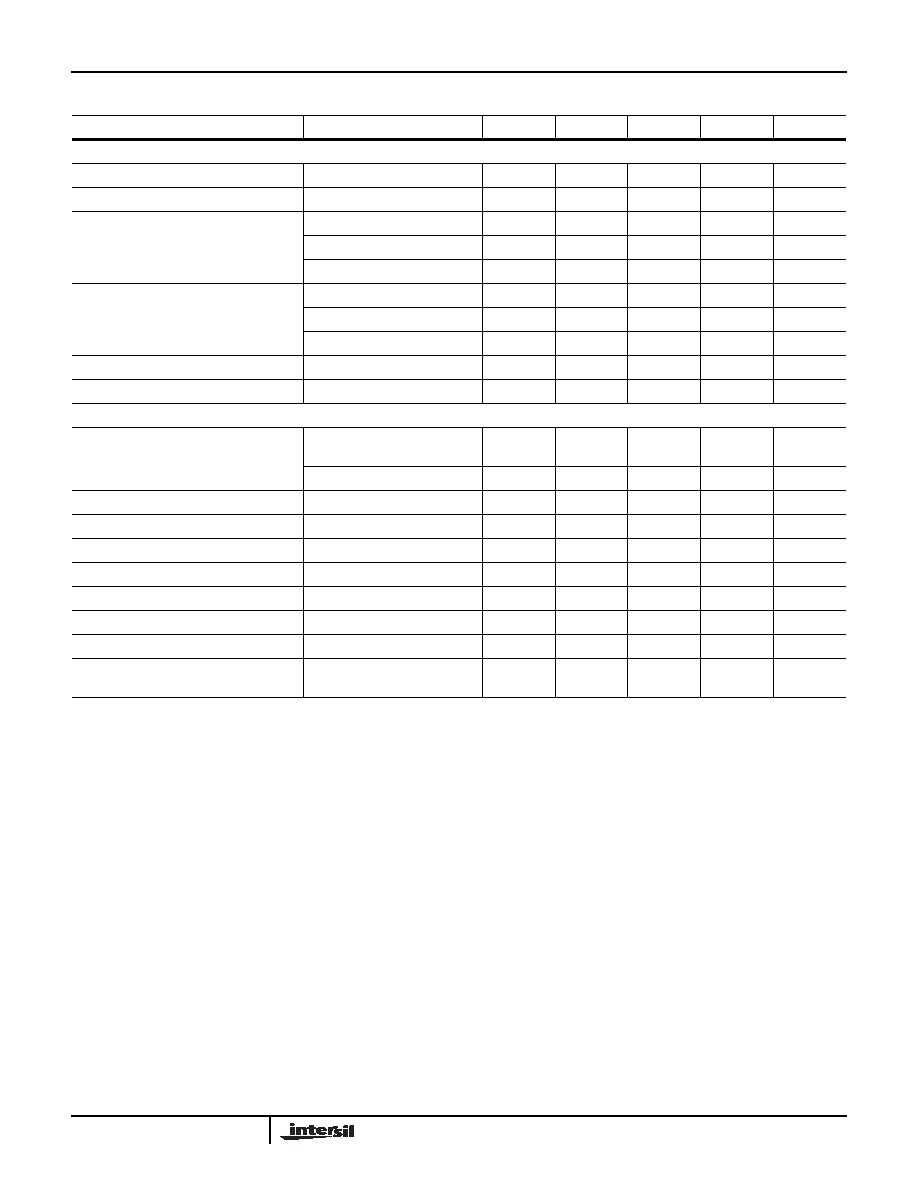
Switching Specifications
PARAMETER
CONDITION
SYMBOL
MIN
TYP
MAX
UNITS
ADC OUTPUT
Aperture Delay
tA
375
ps
RMS Aperture Jitter
jA
60
fs
Output Clock to Data Propagation Delay,
LVDS Mode
(Note 9)
DDR Rising Edge
tDC
-260
-50
120
ps
DDR Falling Edge
tDC
-160
10
230
ps
SDR Falling Edge
tDC
-260
-40
230
ps
Output Clock to Data Propagation Delay,
CMOS Mode
(Note 9)
DDR Rising Edge
tDC
-220
-10
200
ps
DDR Falling Edge
tDC
-310
-90
110
ps
SDR Falling Edge
tDC
-310
-50
200
ps
Latency (Pipeline Delay)
L
8.5
cycles
Overvoltage Recovery
tOVR
1cycles
SPI INTERFACE (Notes 10, 11)
SCLK Period
Write Operation
t
CLK
16
cycles
(Note 10)
Read Operation
tCLK
66
cycles
SCLK Duty Cycle (tHI/tCLK or tLO/tCLK)
Read or Write
25
50
75
%
CSB
↓ to SCLK↑ Setup Time
Read or Write
tS
1cycles
CSB
↑ after SCLK↑ Hold Time
Read or Write
tH
3cycles
Data Valid to SCLK
↑ Setup Time
Write
tDSW
1cycles
Data Valid after SCLK
↑ Hold Time
Write
tDHW
3cycles
Data Valid after SCLK
↓ Time
Read
tDVR
16.5
cycles
Data Invalid after SCLK
↑ Time
Read
tDHR
3cycles
Sleep Mode CSB
↓ to SCLK↑ Setup Time
(Note 12)
Read or Write in Sleep Mode
tS
150
s
NOTES:
8. The Tri-Level Inputs internal switching thresholds are approximately 0.43V and 1.34V. It is advised to float the inputs, tie to ground or AVDD
depending on desired function.
9. The input clock to output clock delay is a function of sample rate, using the output clock to latch the data simplifies data capture for most
applications. Contact factory for more info if needed.
10. SPI Interface timing is directly proportional to the ADC sample period (tS). Values above reflect multiples of a 4ns sample period, and must be
scaled proportionally for lower sample rates.
11. The SPI may operate asynchronously with respect to the ADC sample clock
12. The CSB setup time increases in sleep mode due to the reduced power state, CSB setup time in Nap mode is equal to normal mode CSB setup
time (4ns min).
KAD5512HP
发布紧急采购,3分钟左右您将得到回复。
相关PDF资料
KAD5512P-17Q72
IC ADC 12BIT 170MSPS SGL 72-QFN
KAD5514P-12Q72
IC ADC 14BIT 125MSPS SGL 72-QFN
KAD5610P-25Q72
IC ADC 10BIT 250MSPS DUAL 72-QFN
KAD5612P-17Q72
IC ADC 12BIT 170MSPS DUAL 72-QFN
LA72715NV-TLM-E
IC AUDIO DECODER JPN MTS 24SSOP
LICAL-DEC-LS001
IC DECODER LOW SECURITY 8DIP
LICAL-DEC-MS001
IC DECODER MS SERIES 20-SSOP
LICAL-ENC-MS001
IC ENCODER MS SERIES 20-SSOP
相关代理商/技术参数
KAD5512HP-21Q48
功能描述:模数转换器 - ADC 12-BIT 210MSPS HI PERF SINGLE ADC PROG
RoHS:否 制造商:Texas Instruments 通道数量:2 结构:Sigma-Delta 转换速率:125 SPs to 8 KSPs 分辨率:24 bit 输入类型:Differential 信噪比:107 dB 接口类型:SPI 工作电源电压:1.7 V to 3.6 V, 2.7 V to 5.25 V 最大工作温度:+ 85 C 安装风格:SMD/SMT 封装 / 箱体:VQFN-32
KAD5512HP-21Q72
功能描述:模数转换器 - ADC 12-BIT 210MSPS HI PERF SINGLE ADC PROG
RoHS:否 制造商:Texas Instruments 通道数量:2 结构:Sigma-Delta 转换速率:125 SPs to 8 KSPs 分辨率:24 bit 输入类型:Differential 信噪比:107 dB 接口类型:SPI 工作电源电压:1.7 V to 3.6 V, 2.7 V to 5.25 V 最大工作温度:+ 85 C 安装风格:SMD/SMT 封装 / 箱体:VQFN-32
KAD5512HP-25Q48
功能描述:模数转换器 - ADC 12-BIT 250MSPS HI PERF SINGLE ADC
RoHS:否 制造商:Texas Instruments 通道数量:2 结构:Sigma-Delta 转换速率:125 SPs to 8 KSPs 分辨率:24 bit 输入类型:Differential 信噪比:107 dB 接口类型:SPI 工作电源电压:1.7 V to 3.6 V, 2.7 V to 5.25 V 最大工作温度:+ 85 C 安装风格:SMD/SMT 封装 / 箱体:VQFN-32
KAD5512HP-25Q72
功能描述:模数转换器 - ADC 12-BIT 250MSPS HI PERF SINGLE ADC
RoHS:否 制造商:Texas Instruments 通道数量:2 结构:Sigma-Delta 转换速率:125 SPs to 8 KSPs 分辨率:24 bit 输入类型:Differential 信噪比:107 dB 接口类型:SPI 工作电源电压:1.7 V to 3.6 V, 2.7 V to 5.25 V 最大工作温度:+ 85 C 安装风格:SMD/SMT 封装 / 箱体:VQFN-32
KAD5512P
制造商:INTERSIL 制造商全称:Intersil Corporation 功能描述:Low Power 12-Bit, 250/210/170/125MSPS ADC
KAD5512P_09
制造商:INTERSIL 制造商全称:Intersil Corporation 功能描述:Low Power 12-Bit, 250/210/170/125MSPS ADC
KAD5512P-12Q48
功能描述:模数转换器 - ADC 12-BIT 125MSPS SINGL ADC PROG LVDS/LVCMOS RoHS:否 制造商:Texas Instruments 通道数量:2 结构:Sigma-Delta 转换速率:125 SPs to 8 KSPs 分辨率:24 bit 输入类型:Differential 信噪比:107 dB 接口类型:SPI 工作电源电压:1.7 V to 3.6 V, 2.7 V to 5.25 V 最大工作温度:+ 85 C 安装风格:SMD/SMT 封装 / 箱体:VQFN-32
KAD5512P-12Q72
功能描述:模数转换器 - ADC 12-BIT 125MSPS SINGL ADC PROG LVDS/LVCMOS RoHS:否 制造商:Texas Instruments 通道数量:2 结构:Sigma-Delta 转换速率:125 SPs to 8 KSPs 分辨率:24 bit 输入类型:Differential 信噪比:107 dB 接口类型:SPI 工作电源电压:1.7 V to 3.6 V, 2.7 V to 5.25 V 最大工作温度:+ 85 C 安装风格:SMD/SMT 封装 / 箱体:VQFN-32